3DCSI
Welcome at the Website of the ESF Young investigators Group "3D Chip Stack Intraconnects - 3DCSI"!
[Motivation and Goal] [Participating Groups] [Project Duration] [Funding]
Motivation and Goal
Dresden has become the largest microelectronics hub in Europe during the last decades. Leading industry like Globalfoundries and Infineon as well as the TU Dresden and the regional non-university research institutes shape the outstanding innovation power of the region which also impacts the employment market in this high-tech area having reached 50,000 employees in 2011. Microelectronics is the driving force behind a myriad of innovations pushing economy and society, and 3D integration of chip stacks is expected to be the next fundamental innovation push for microelectronics. With the upcoming 3D integration of several chips into a vertical stack many challenges have surfaced which need to be addressed before 3D integration technology can be deployed in the mainstream.
One of the most promising aspects of 3D integration is the ability to integrate, at the wafer level, heterogeneous layers in the same vertical stack. This heterogeneity can be used to achieve very high-levels of integration, resulting in very-small form factors, and to implement low-power, high data-rate systems that can overcome bandwidth and area bottlenecks. Examples of such systems include
- 2D imagers with fully parallel analog-to-digital conversion;
- multi-core processors with on-chip photonics communication fabric;
- arrays of MEMS sensors (piezoelectric or capacitive) stacked right above their supporting IC processors;
- compute/sensing nodes integrated with their own solar energy harvesters using high-efficiency solar cells in the 3D stack.
In the case of silicon photonics, 3D heterogeneous integration provides the opportunity of integrating compact laser sources that use materials with tunable index of refraction such as Chalcogenide glass. In imaging applications, 3D heterogeneous integration enables the use of SiGe/Ge photo-detectors as the front end of a Si-based AMS and DSP chip. Furthermore, in wireless communication applications, 3D heterogeneous integration enables the decoupling of the analog domain and the digital domain, thus contributing to the elimination of substrate noise impact on the analog front end. To reap the full benefit of the high bandwidth provided by the TSVs (through silicon vias), new ways of architecting and partitioning 2D integrated circuits among the different 3D layers will have to be devised.
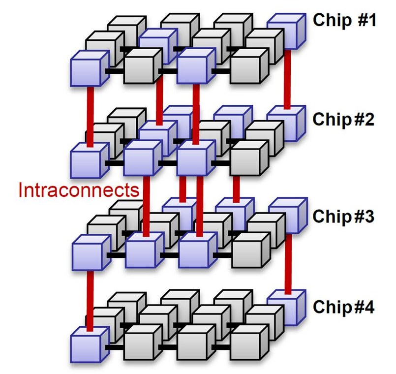
The research of the Young Investigators Group "3D Chip Stack Intraconnects" is focused on the intraconnect aspects of 3D integration, especially the crucial role of TSV in the back-end-of-the-line structure of 3D stacked chips. The goal is to develop modules (design blocks) for high-rate interfaces between multiple chips in a semiconductor chip-stack. These interfaces need to be well adapted to the material properties as well as to the line routing in the chip-stack. To reach the goal, the project will investigate the interfaces and line routing for high-speed communication networks in 3D integrated chips. This includes a thorough characterization of possible interface techniques (copper lines, optical wave guides, and wireless coupling), different semiconductor technologies (SOI, SiGe, etc.) and two types of TSVs (face-to-face and back-to-face). Regarding the TSV fabrication, one of the main challenges will be to cope with several limits that result from the particular properties of the different materials and from the integration technology for the structuring and coating processes.
Participating Groups
Prof. Gerhard Fettweis, Vodafone Chair Mobile Communications Systems
Prof. Johann W. Bartha, Institute of Semiconductors and Microsystems, Chair for Semiconductor Technology
Prof. Dirk Plettemeier, Chair for RF Engineering
Prof. Rene Schüffny, Chair of Highly-Parallel VLSI-Systems and Neuromorphic Chips
Prof. Frank Ellinger, Chair for Circuit Design and Network Theory
Jun.-Prof. Kambiz Jamshidi, Chair for RF Engineering
Project Duration
01.03.2012 - 31.12.2014
Funding
The project is funded by the Free State of Saxony through funds from the European Commission - European Social Funds.