novel types of semiconducting materials
Condensed matter physics is a fascinating branch of physical sciences that allows us to study and understand the matter that surrounds us. One particular category of matter, namely semiconductors, have revolutionised our life as their integration into electronic and optoelectronic devices facilitated the development of numerous technological advances. The vast majority of these devices are based on crystalline, highly ordered systems such as Si and GaAs, the physics of which is well understood after extensive research over the last seven decades. Additionally, these devices begin to reach the limits of their potential performance as exemplified by Moore’s law and the Shockley–Queisser limit. Future generations of electronic and optoelectronic devices will depend on our ability to design novel types of semiconducting materials with new properties, physics and applications.
 © Amac Garbe
novel types of semiconducting materials
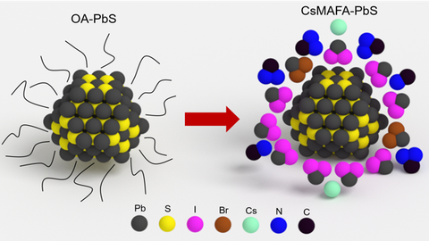
The Emerging Electronic Technologies Chair focuses on the study of such novel semiconducting materials, which greatly vary in their structure, dimensionality and degree of order. Specifically, our expertise ranges from inorganic quantum dot materials to polycrystalline hybrid organic-inorganic perovskites to highly disordered soft organic systems. These versatile material classes are processed from solution at very low temperatures, yet they all demonstrate excellent optoelectronic properties, exciting solid-state physics and photophysics and promising performance in a range of electronic devices. The imperfect nature of these materials results also in a rich defect physics with fascinating implications on the material properties. Additionally, the interaction of defects with light or environmental factors such as O2 and H2O greatly influences the physics of material degradation, but also reveals exotic and highly desirable properties such as material healing.
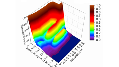
To investigate the properties of these materials we apply a broad range of microscopic and spectroscopic methods. Within the latter, our expertise lies in photoemission, photothermal deflection and photoluminescence spectroscopies, which combined with device fabrication and characterisation provide us meaningful insights into the material physics and light-matter interactions in these novel semiconductor materials. We use devices as a tool to investigate the desired properties of the material and routinely fabricate field-effect transistors, photovoltaic and light-emitting diodes to complement the fundamental characterisation of materials by spectroscopy. Beyond the application of existing methods, we work on the development of new experimental methodologies based on photoemission and photothermal deflection spectroscopies. For example, we recently developed a novel ultraviolet photoemission depth profiling method that allows probing the electronic structure at the bulk of materials and across multi-layers.


