10.11.2017
Can solids wet surfaces?
Wettability of surfaces affects several natural phenomena and plays a crucial role in practical applications such as printing, adhesion, lubrication, etc. Several thin-films made of organic and inorganic materials tend to break-up in small drops when processed at high temperatures, still lower than their melting point. This unstable behavior, usually referred to as dewetting, is common also for crystalline solids, such as metals and semiconductors, and it has been deeply investigated in the last 60 years. The reason of this interest mostly lies in the limit imposed by such a spontaneous phenomenon to the miniaturization of microelectronic devices (e.g. silicon-based transistor) and their electric contacts. Due to their instability, the maximum temperature to process silicon thin-films is usually a few hundred Celsius and it has been mostly addressed as an issue for several applications.
However, the control over the size and the shape of silicon self-assembled structures allows for the tuning of surface properties leading to interesting applications. For instance, silicon particles with a size smaller than one micron allow for an efficient manipulation of the incident light on a substrate making it anti-reflective or perfectly reflective according to conditions (e.g. shape and distance of the particles). Therefore, controlling the formation of small silicon particles with controlled shape and density by means of a simple thermal treatment would open the possibility to obtain cheap, large-scale dielectric meta-surfaces.
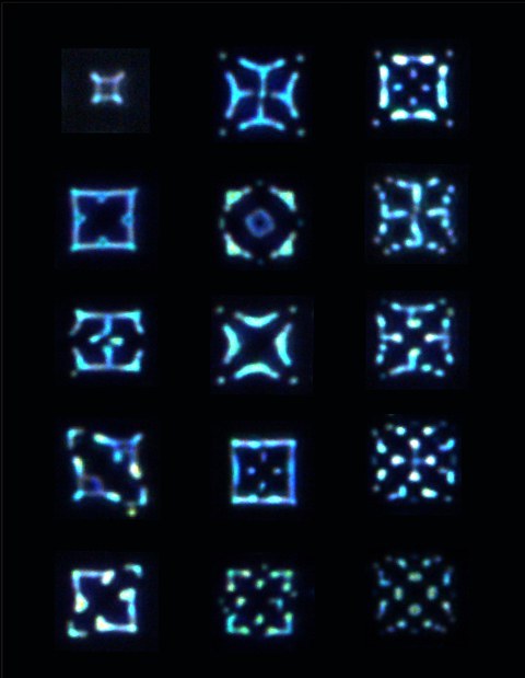
In this work, we showed for the first time how to control the formation of complex nano-architectures made of single-crystal silicon on silicon dioxide. In analogy with what obtained for metals, it is actually possible to drive the dewetting front of a thin-film thanks to a lithographic patterning of the sample. By means of high-temperature treatment (~740 °C) under vacuum (~10-10 Torr), the material arranged in squared patches with a thickness of 12 nm and a high-to-base aspect-ratio ~1/400, is precisely redistributed over a few microns.
A crucial part of this work dealt with the theoretical modeling of the self-assembly process observed during the dewetting of silicon. Thanks to continuum modeling, the optimisation of advanced computational techniques and simulations exploiting high-performance computing, a theoretical approach able to predict the dynamics during the process has been developed. This allows for testing a priori the lithographic patterning and predicting the morphological evolution up to the final shape. Therefore, it will be possible to select a specific patterning prior to experiments in order to obtain a complex architecture with a morphology targeted for specific applications.
Finally, not all the materials can be manipulated efficiently at the nanoscale, neither with this approach nor with other techniques. Therefore, exploiting a sol-gel dip-coating technique combined with nanoimprint, the complex morphologies obtained with silicon have been adopted as a master and transferred to other materials as titanium and silicon oxides. This opens the possibility to select the substrate on which the nano-architectures will be printed and also to control the porosity of the materials. A crucial feature of this shape-transfer technique is the very low temperature (~400 °C), that makes it fully compatible with C-MOS electronic devices.
The applications of this study will be strictly related to the fine control of the morphologies, their large size, and their reproducibility. For silicon on silicon dioxide, they involve the integration of dielectric material in microelectronics and photonics (e.g. nano-circuits, meta-surfaces, waveguides, optical interferometers, etc ..). Applications of structures made of titanium and silicon dioxides deal with dielectric meta-surfaces, microfluidics, sensors or biomedical applications.
Original Publication:
“Complex dewetting scenarios of ultrathin silicon films for large-scale nanoarchitectures” in Science Advances (online)
Reference:
Naffouti et al., Sci. Adv. 2017; 3 : eaao1472
CONTACTS:

