Atomically-thin materials
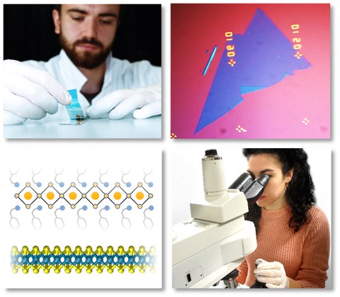
Van der Waals crystals with active layers being as thin as just a few atoms are of major interest for solid state physics research. They represent the ultimate two-dimensional limit for matter, exhibiting a variety of intriguing properties and emerging phenomena. In addition, the possibility to artificially design heterostructures with novel degrees of freedom and opportunities for environmental engineering offer promising avenues for future optoelectronic technologies.
In our studies we employ a variety of two-dimensional semiconductors including the family of transition metal dichalcogenides [1] and organic-inorganic hybrid perovskites [2]. We fabricate heterostructures to modify energy landscapes for optoelectronic excitations through dielectric [3] or strain engineering [4], controlling disorder [5] or providing electrical tunability [6]. In our focus are combinations of atomically-thin crystals with one- and zero-dimensional nanostructures and their behavior in the presence of strong external fields [7, 8].
[1] K. Wagner et al. Phys. Rev. Lett. 127, 076801 (2021) https://doi.org/10.1103/PhysRevLett.127.076801
[2] J. D. Ziegler et al. Nano Lett. 20, 6674 (2020) https://doi.org/10.1021/acs.nanolett.0c02472
[3] A. Raja et al. Nature Commun. 8, 15251 (2017) https://doi.org/10.1038/ncomms15251
[4] F. Dirnberger & J. D. Ziegler et al. Science Adv. 7, eabj3066 (2021) https://www.science.org/doi/full/10.1126/sciadv.abj3066
[5] A. Raja et al. Nature Nanotech., 14, 832 (2019) https://doi.org/10.1038/s41565-019-0520-0
[6] K. Wagner & E. Wietek et al. Phys. Rev. Lett. 125, 267401 (2020) https://doi.org/10.1103/PhysRevLett.125.267401
[7] A. Chernikov & C. Ruppert et al. Nature Photon., 9, 466 (2015) https://doi.org/10.1038/nphoton.2015.104
[8] J. Zipfel et al. Phys. Rev. B 98, 075438 (2018) https://doi.org/10.1103/PhysRevB.98.075438

