Joint research activities of TU Dresden (Institute of Semiconductors and Microsystems) and NaMLab gGmbH

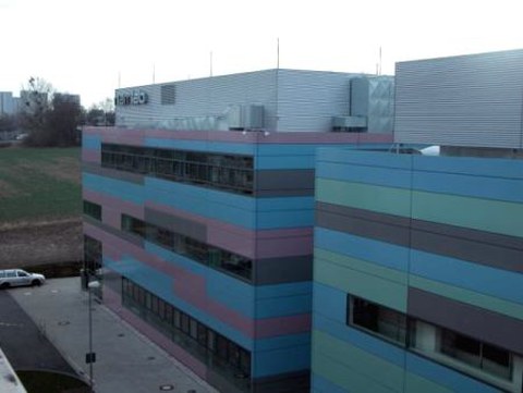
NaMLab gGmbH building next to the cleanroom building at MIERDEL-Bau
On October 15th in 2007 the NaMLab was solemnly opened. Until the end of the year a large part of the technical devices could be finished. In parallel the installation of the facilities has started. Those facilities are used particularly for the deposition of insulator-materials by use of MBE, Magnetronsputtern and ALD. Furthermore corresponding equipments for the material characterization were established.
The Institute of Semiconductors and Microsystems together with the NaMLab have build up a technological chain for producing test-structures for material screening of insulator materials with a preferably high relative permittivity (high-k), that is suitable for application in microelectronic components. For this purpose a research project sponsored by BMBF was initiated (see project KONDOR).
Research emphasis
The NaMLab gGmbH develops production methods and methods of characterization for nanoelectronical materials that, aside of microelectronics, can also be applied in other areas like for exaple in photovoltaics. First research emphasis were the studies of suitable materials for advanced silicon-technologies. Those are in particular
- research activities for new materials as replacement for SiO2 as dielectric medium,
- the associated metal electrodes as well as
- foundational researches for the integration of materials or nanostructures in silicon as a possible replacement for conventional transistor channels.
