Angebote und Dienstleistungen
Die an der Professur Nanoelektronik vorhandenen Techniken und Technologien der Mikroelektronik, der Mikrosystemtechnik und Sensorik stehen auch lehrstuhlfremden Mitarbeitern der TU Dresden und Einrichtungen bzw. Firmen außerhalb der TU Dresden zur Verfügung. Die Erarbeitung und Realisierung kundenspezifischer Lösungen steht dabei im Vordergrund.
Anhand einiger Beispiele werden diese Forschungsdienstleistungen illustriert:
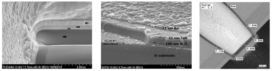
Waferbeschichtungen (Oxidation, PECVD-, ALD- und PVD-Prozesse für Herstellung funktionaler Schichten und Schichtsysteme, Diffusionsbarrieren, Metallisierungen verschiedener Einsatzbereiche)
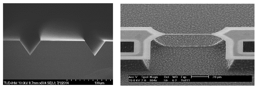
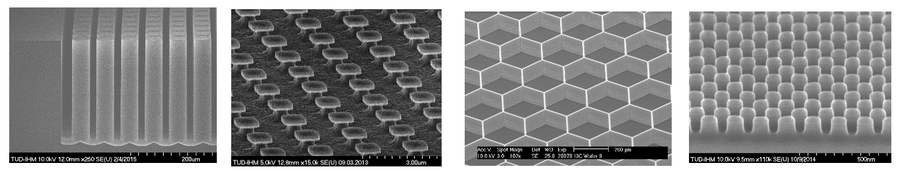
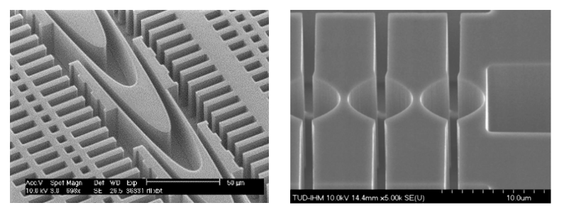
Schichtstrukturierung (chemisches Naß- und Trockenätzen)
Trennschleifen verschiedener Substrate (max. 200mm Durchmesser) und Substratmaterialien (Si, Saphir, Gläser)
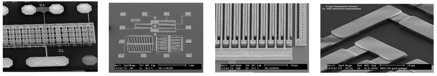
Additive und subtraktive Verdrahtungstechnologien (Damascene Strukturierung)
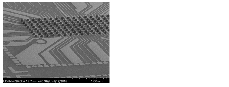
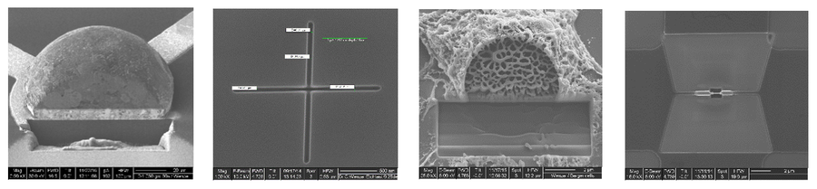
Waferbumping
Si-Tiefenätzen für MEMS, MOEMS und Mikrofluidik
Röntgennanolinsen
Dünnschichtkondensatoren
Elektrische Messtechniken (C-V, I-V, Durchbruch, TVS, Charakterisierung von Solarzellen) z.B. Vakuumprober für Feuchtigkeits- und Wärmetests
Focused Ion Beam
Am Anfang solcher Arbeiten stehen eine intensive Diskussion und Beratung zu den Zielen und den Realisierungsmöglichkeiten. Bei Bedarf werden Vorversuche durchgeführt, die das Risiko eines Scheiterns minimieren sollen. Danach erfolgt in der Regel ein verbindliches Angebot zu den Kosten, die sich aus den tatsächlichen Kosten und einem Unizuschlag zusammensetzen. Es gelten die Allgemeinen Geschäftsbedingungen der TU Dresden. Die Forschungsdienstleistungen werden nach bestem Fachwissen ausgeführt, eine Ergebnishaftung kann jedoch nicht gegeben werden.
Weitere Informationen und Anfragen: