Applications of semiconductor nanomatrials
The chemistry of colloidal NCs has already matured during last decades to the level, where a wide variety of high quality materials can easily be produced by a plethora of synthetic protocols developed to date. Thus, now it is time to turn semiconductor NCs to practical applications, for example as active materials in various optoelectronic devices. Being soluble objects, semiconductor NCs can be processed via common solution-based techniques, such as drop-casting; spin-, dip-, and spray-coating; and inkjet printing, transfer printing, and imprinting. Most of their optoelectronic applications, e.g., in light-emitting diodes (LEDs), solar cells, photodetectors, and field-effect transistors (FETs), involve NC-based solids, typically in the form of thin films. In color-conversion layers (used, for example, in TV screens) and in luminescent solar concentrators, they are applied in the form of NCs-in-polymer composites. For most of these applications, as-prepared NCs should undergo additional post-synthetic treatment.
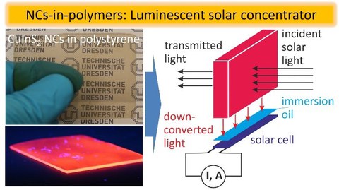
Abb 7. NCs for luminescent solar concentrators. Copyright 2017, Wiley-VCH GmbH (ref. 12)
We develop strategies to incorporate various NCs into polymer matrices aiming at transparent brightly luminescent composite materials. These composites can be prepared either in the form of thin films deposited on different substrates or in the form of bulks, depending on the method of the composite fabrication. For example, a special design of the surface of Cu-In-S NCs allowed us to prepare transparent and photostable NCs-in-polymer composites tested as luminescent solar concentrators.12 In order to improve compatibility of the NCs with the polymer matrix, they were modified by anchoring copolymerizable molecules. In close collaboration with the group of Prof. S. V. Kostjuk (Belarusian State University) we develop novel composites of semiconductor NCs in cross-linking polyisobutilene-based matrices, characterized by exceptional photo- and chemical stability.13-14
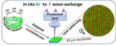
Abb 8. NCs in polymers for microdisplays.
Green and red color pixels can directly be patterned with 15 µm resolution in a polymer matrix containing perovskite NCs upon pulsed UV-laser irradiation (in collaboration with Prof. L. Orazi, Uni. Modena and Reggio, Italy).15 This process is based on an in-situ anion exchange reaction transforming green-emitting CsPbBr3 NCs into red-emitting CsPbI3 perovskite NCs. This method opens up great opportunities in flexible production of small- and mid-size batches of display devices.
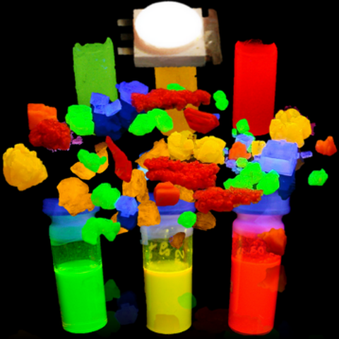
Abb 9. NCs in salt crystals for LEDs
Another example of composite materials is NCs-in-salt crystals. Embedding NCs into crystalline host matrixes, such as ionic salts of NaCl, KCl, borax, etc., is a step forward for superior photostability, thermal stability, and chemical durability of NC-based luminophores while simultaneously sustaining high quantum yields. We introduced and investigated several basic methods for loading the salt macrocrystals with NCs, namely relatively slow direct embedding, as well as accelerated methods of vacuum-, pressure- and liquid−liquid diffusion-assisted crystallization. We investigated photophysical properties of the resulting composites and validated them for application in light-emitting diodes as well as in the fields of plasmonics and excitonics.16-21
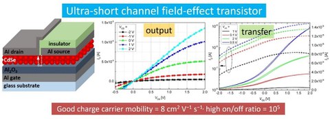
Semiconductor NCs being processed in the form of thin films, typically with a thickness on the order of hundred nanometers, are integrated into FETs and photodetectors. Here, in order to improve charge transport within the films the NCs are ligand exchanged with compact inorganic ions, such as S2– or Br–. A novel FET device architecture has been employed to construct a high-performance ultra-short channel FET in close collaboration with the group of Dr. H. Kleemann (Dresden Integrated Center for Applied Photophysics and Photonic Materials).22 Employing photolithographic methods combined with spin-coating, we fabricated FETs with a vertical overlap of source and drain electrodes to achieve a submicrometer channel length. The device exhibits good transport characteristics with electron mobilities in the saturation regime reaching 8 cm2 V–1 s–1 and a high on/off ratio of 105.
Abb 10. NCs in FETs
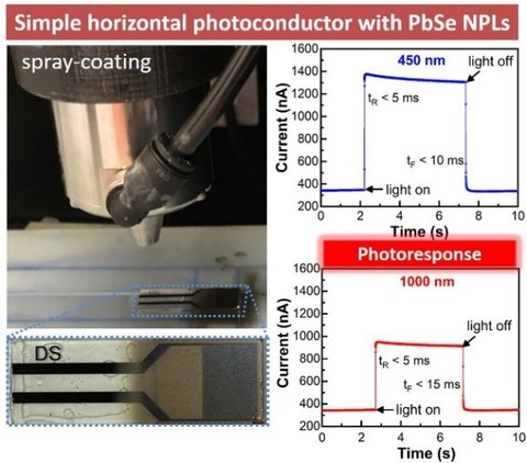
Abb 11. NCS in photodetectors.
Among photodetectors especially interesting are those devices which are able to respond to light in a broad wavelength range, e.g. from visible to the NIR. Starting from NIR-active PbSe NPLs we fabricated simple photodetectors using commercially available electrodes.23 Spray-coating of the NPL dispersions under ambient conditions with no additional treatment resulted in photodetectors with excellent responsivity to both visible (450 nm) and NIR (1000 nm) light at low operational voltages. This work clearly demonstrates a great potential of the developed methods to manufacture large-area optoelectronic devices.
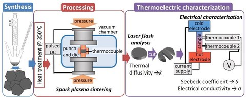
Abb 12. NCs for thermoelectrics.
In close collaboration with the group of Prof. K. Nielsch (Leibniz Institute for Solid State and Materials Research Dresden) we develop efficient nanostructured thermoelectric materials – semiconductor compounds with a narrow bandgap able to transform thermal energy (i.e. temperature gradient over such bulk piece of the material) into electricity. One of the classic thermoelectric compounds with high efficiency is Bi2Te3. Specially designed heterostructured core/shell Bi2Te2Se/Bi2Te3 nanosheets processed via spark-plasma sintering into nanostructured pellets exhibited an excellent performance with a very high zT value (a figure of merit characterizing thermoelectrics) over 1.34 at 400 K.24
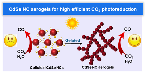
Semiconductor NCs are one of the most attractive photocatalyst due to their many excellent photoelectronic properties, including high molar extinction coefficients, tunable band gaps, as well as abundant surface sites. However, the well-dispersed colloidal NCs suffer from low CO adsorption capacity and poor charge separation efficiency. The drawbacks mentioned above limit the wide application of colloidal NC photocatalysts. Herein, we prepared novel CdSe NC aerogels with 3D selfsupported architecture for visible-light-driven CO2 reduction. The NC aerogels exhibit superior photocatalytic performance in gas-phase CO2 reduction at ambient pressure.25
Abb 13. NC aerogels in photocatalysis.
References
12. Lesyuk, R.; Cai, B.; Reuter, U.; Gaponik, N.; Popovych, D.; Lesnyak, V., Quantum-Dot-in-Polymer Composites via Advanced Surface Engineering. Small Methods 2017, 1 (9), 1700189.
13. Prudnikau, A.; Shiman, D. I.; Ksendzov, E.; Harwell, J.; Bolotina, E. A.; Nikishau, P. A.; Kostjuk, S. V.; Samuel, I. D. W.; Lesnyak, V., Design of cross-linked polyisobutylene matrix for efficient encapsulation of quantum dots. Nanoscale Adv. 2021, 3 (5), 1443-1454.
14. Shiman, D. I.; Sayevich, V.; Meerbach, C.; Nikishau, P. A.; Vasilenko, I. V.; Gaponik, N.; Kostjuk, S. V.; Lesnyak, V., Robust Polymer Matrix Based on Isobutylene (Co)polymers for Efficient Encapsulation of Colloidal Semiconductor Nanocrystals. ACS Appl. Nano Mater. 2019, 2 (2), 956-963.
15. Martin, C.; Prudnikau, A.; Orazi, L.; Gaponik, N.; Lesnyak, V., Selectively Tunable Luminescence of Perovskite Nanocrystals Embedded in Polymer Matrix Allows Direct Laser Patterning. Adv. Optical Mater. 2022, 2200201.
16. Otto, T.; Müller, M.; Mundra, P.; Lesnyak, V.; Demir, H. V.; Gaponik, N.; Eychmüller, A., Colloidal Nanocrystals Embedded in Macrocrystals: Robustness, Photostability, and Color Purity. Nano Lett. 2012, 12 (10), 5348-5354.
17. Adam, M.; Erdem, T.; Stachowski, G. M.; Soran-Erdem, Z.; Lox, J. F. L.; Bauer, C.; Poppe, J.; Demir, H. V.; Gaponik, N.; Eychmüller, A., Implementation of High-Quality Warm-White Light-Emitting Diodes by a Model-Experimental Feedback Approach Using Quantum Dot–Salt Mixed Crystals. ACS Appl. Mater. Interfaces 2015, 7 (41), 23364-23371.
18. Adam, M.; Wang, Z.; Dubavik, A.; Stachowski, G. M.; Meerbach, C.; Soran-Erdem, Z.; Rengers, C.; Demir, H. V.; Gaponik, N.; Eychmüller, A., Liquid–Liquid Diffusion-Assisted Crystallization: A Fast and Versatile Approach Toward High Quality Mixed Quantum Dot-Salt Crystals. Adv. Funct. Mater. 2015, 25 (18), 2638-2645.
19. Adam, M.; Gaponik, N.; Eychmüller, A.; Erdem, T.; Soran-Erdem, Z.; Demir, H. V., Colloidal Nanocrystals Embedded in Macrocrystals: Methods and Applications. J. Phys. Chem. Lett. 2016, 7 (20), 4117-4123.
20. Guhrenz, C.; Benad, A.; Ziegler, C.; Haubold, D.; Gaponik, N.; Eychmüller, A., Solid-State Anion Exchange Reactions for Color Tuning of CsPbX3 Perovskite Nanocrystals. Chem. Mater. 2016, 28 (24), 9033-9040.
21. Benad, A.; Guhrenz, C.; Bauer, C.; Eichler, F.; Adam, M.; Ziegler, C.; Gaponik, N.; Eychmüller, A., Cold Flow as Versatile Approach for Stable and Highly Luminescent Quantum Dot–Salt Composites. ACS Appl. Mater. Interfaces 2016, 8 (33), 21570-21575.
22. Fan, X.; Kneppe, D.; Sayevich, V.; Kleemann, H.; Tahn, A.; Leo, K.; Lesnyak, V.; Eychmüller, A., High-Performance Ultra-Short Channel Field-Effect Transistor Using Solution-Processable Colloidal Nanocrystals. J. Phys. Chem. Lett. 2019, 10, 4025-4031.
23. Galle, T.; Spittel, D.; Weiß, N.; Shamraienko, V.; Decker, H.; Georgi, M.; Hübner, R.; Metzkow, N.; Steinbach, C.; Schwarz, D.; Lesnyak, V.; Eychmüller, A., Simultaneous Ligand and Cation Exchange of Colloidal CdSe Nanoplatelets toward PbSe Nanoplatelets for Application in Photodetectors. J. Phys. Chem. Lett. 2021, 12, 5214-5220.
24. Bauer, C.; Veremchuk, I.; Kunze, C.; Benad, A.; Dzhagan, V. M.; Haubold, D.; Pohl, D.; Schierning, G.; Nielsch, K.; Lesnyak, V.; Eychmüller, A., Heterostructured Bismuth Telluride Selenide Nanosheets for Enhanced Thermoelectric Performance. Small Sci. 2021, 1 (1), 2000021.
25. Jiang, G.; Wang, J.; Li, N.; Hübner, R.; Georgi, M.; Cai, B.; Li, Z.; Lesnyak, V.; Gaponik, N.; Eychmüller, A., Self-Supported Three-Dimensional Quantum Dot Aerogels as a Promising Photocatalyst for CO2 Reduction. Chem. Mater. 2022, 34 (6), 2687-2695

