THE WORKING GROUP INTRODUCES ITSELF
Our research focus is on the optical and electrical properties of crystalline semiconductors and their connection to the lattice structure. Both fundamental and applied questions are examined.

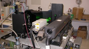
Special equipment
Systems for identifying electrically active defects in semiconductors: DLTS, CV, IV, Hall effect; photoluminescence and Raman scattering at variable temperatures and different laser excitations; Fourier transform infrared absorption and photocurrent spectroscopy for detecting local vibration modes and electronic transitions of defects from far infrared to UV; dc and rf plasma setups for hydrogenation in the temperature
range from RT to 1200°C; a variety of furnaces capable of annealing samples in different ambients from RT up to 1400°C; chemical lab for processing semiconductor samples.

