Motivation
In initial courses on solid state physics, the concept of an ideal crystal is introduced in which each atom occupies a certain place. This, however, is an idealization that is very far from reality. There are no ideal crystals.
Already in the early stages of the solid state research, it was established that defects often have a profound effect on their physical properties. The most impressive examples of this kind can be found in physics of semiconductors. The very existence of semiconductor electronics is based on the ability to control both the magnitude and type of electrical conductivity by introducing small additions of chemical impurities that have the properties of small donors or acceptors.
The study of defects in semiconductors therefore became an area of active research immediately after semiconductors emerged as important technological materials. Moreover, the development of nanoelectronics has led to a significant increase in the vulnerability of devices to unwanted defects arising during material processing. At the same time, due to the development of new devices and technological processes, the requirements for precision control of material properties through the introduction of desired defects have increased.
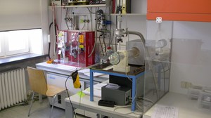
For a long time, our group has been studying the properties of defects in semiconductors ranging from "classical" Si, Ge and GaAs to transparent conducting oxides such as ZnO, SnO2, TiO2, etc. The main research method is optical spectroscopy, including photoluminescence, IR absorption, Raman scattering and photoconductivity. Additional methods include various types of capacitance spectroscopy (DLTS, minority carrier spectroscopy, etc.) and the Hall effect. In addition, we closely collaborate with various theoretical groups. The combination of various experimental methods and in-depth theoretical analysis allows to achieve significant progress in understanding the properties of defects in semiconductors and, consequently, in the development of new semiconductor technologies.
Current projects
Hydrogen in tin (di)oxide (2021-2024, Deutsche Forschungsgemeinschaft, LA 1397/20-1)
Tin dioxide (SnO2) is an important semiconductor widely employed in transparent conductor electronics, solar cells, gas sensors, touchscreens, catalysis, and spintronics. SnO2 reveals only n-type conductivity what seriously limits the amount of possible application. Tin oxide (SnO), on the other hand, only recently received a great deal of attention since the discovery of ambipolar doping. Hydrogen in metal oxides including both SnO2 and SnO is ubiquitous and very difficult to remove from the crystal growth environment and post-growth treatment. Controlling the conductivity of tin (di)oxide thus requires careful control of hydrogen exposure during and after growth. At present understanding of hydrogen properties in both SnO2 and especially SnO at the microscopic level is very limited. The project aims at bridging this gap. Spectroscopic methods will be employed to get insight into the structural and electrical properties of hydrogen with an emphasis on interstitial species, hydrogen trapped at the oxygen vacancy, hydrogen molecule, and hydrogen-acceptor complexes such as the Sn vacancy passivated by hydrogen.
Shallow dopants and compensating centers in antimony chalcogenides (2023-2026, Deutsche Forschungsgemeinschaft, LA 1397/21-1)
The urgent need for high-efficiency, low-cost solar cells motivates researchers to look for new absorber materials for thin-film photovoltaics. Antimony triselenide (Sb2Se3) and antimony trisulfide (Sb2S3) have attracted immense research interest as new absorber for highly efficient, environmentally friendly, stable, and cost-effective thin-film solar cells. Defects and impurities have a decisive impact on the performance of all semiconductor devices. At present, the physics of defects in Sb2Se3 and Sb2S3 remains unexplored and it is not
ambiguously clear which of native defects, impurities, or defect complexes and to what extend introduce charge carriers and act as detrimental trap sites or recombination centers. The central goal of our project is to study fundamental properties of shallow dopants and compensating centers in single-crystalline Sb2Se3 and Sb2S3. We will focus on technologically important impurities such as chlorine, oxygen, and hydrogen. Optical and electrical spectroscopy will be employed to get insight into microscopic structure, electrical activity, thermal stability, diffusion mechanisms, evolution kinetics, and formation of complexes between extrinsic dopants and native defects. The project will contribute to a better understanding of defects in Sb2Se3 and Sb2S3 and, thus, support efforts in bringing these materials to a broader technological usage in photovoltaics, photoelectrochemical cells, or other solar-driven applications.

