Processing techniques and experimental methods
At the Chair for Organic Semiconductors, we have access to various processing techniques allowing to fabricate any relevant material system. In detail, those methods are:
- Physical vapor deposition of small molecules, metals, and metal oxides in high vacuum
- Sputtering and atomic layer deposition (ALD) of oxides
- Wet-processing of small molecules and polymers (spin coating, spraying, and other coating techniques)
- 3D printing of polymer-based systems
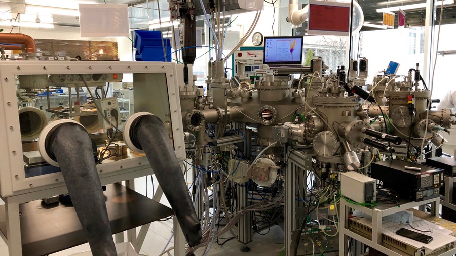
Deposition system to fabricate thin small molecule-based layers
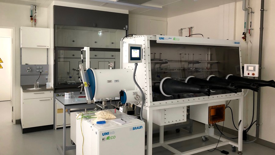
Glovebox and fume hood to process layers by wet-processing techniques
Additionally, we use various experimental methods to prove the properties of our samples and devices. In particular those methods are:
- Basic characterization of OLEDs (Current-Voltage-Luminance characteristics, external quantum efficiency based on integration sphere measurements, OLED lifetime measurements, angular resolved electroluminescence, time resolved electroluminescence)
- Scanning force microscopy and profilometry
- Ellipsometry
- Photoluminescence Quantum Yield in the Range from 380 to 780 nm (for thin films and liquid solutions)
- Angular resolved photoluminescence
- Time- and spectrally resolved spectroscopy (using time correlated single photon counting (TCSPC) [for nanosecond resolution] and fast photodiodes [for millisecond resolution])
- Measurement of device parameters (current, voltage, emitted light) as a function of temperature in a cryostate with Peltier-cooling
- Measurements under different environments using a gas mixing station
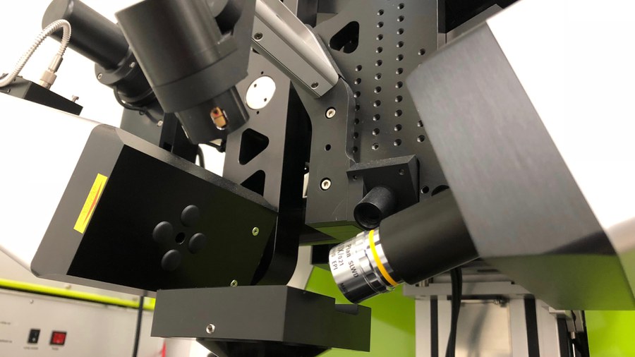
Ellipsometer