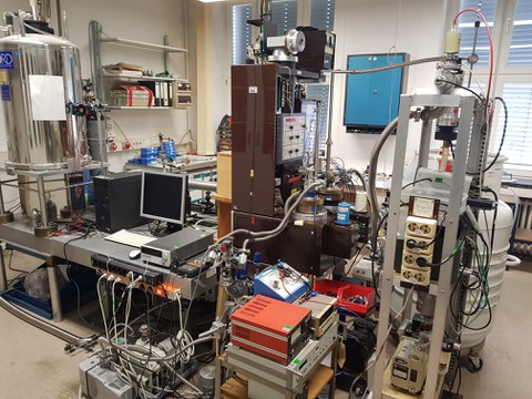
Special equipment
Systems for identifying electrically active defects in semiconductors: DLTS, CV, IV, Hall effect; photoluminescence and Raman scattering at variable temperatures and different laser excitations; Fourier transform infrared absorption and photocurrent spectroscopy for detecting local vibration modes and electronic transitions of defects from far infrared to UV; dc and rf plasma setups for hydrogenation in the temperature
range from RT to 1200°C; a variety of furnaces capable of annealing samples in different ambients from RT up to 1400°C; chemical lab for processing semiconductor samples.

