Chipentwürfe 2011 bis 2015
Inhaltsverzeichnis
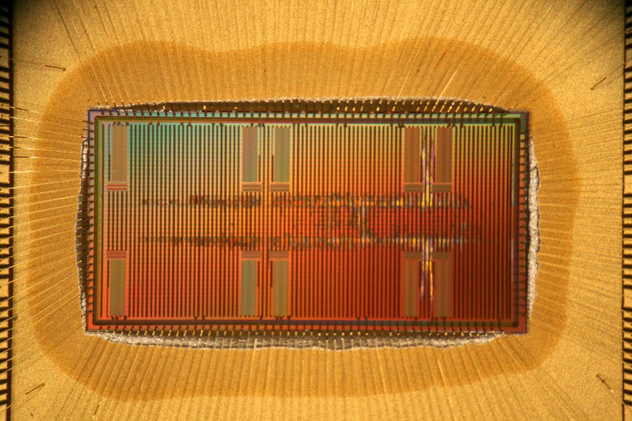
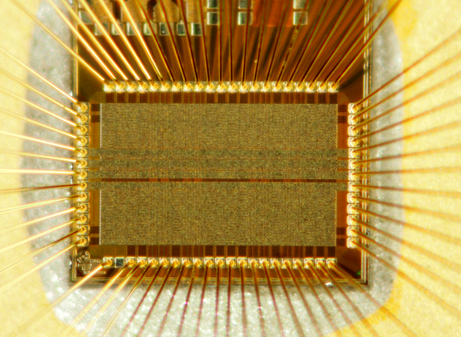
Atlas_Chip
MPSoC with two vector DSP cores. Ultra-fast DVFS for dynamic power management. DDR2 memory interface and high-speed serial NoC links with 36 Gbit/s data rate.
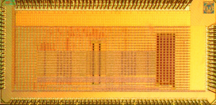
Chipfoto ATLAS_Chip
| Technologie | 65 nm CMOS |
| Area | 7,4 mm² |
| Tape-Out | 03_2011 |
|
Publikationen |
DOI: 10.1109/ISSCC.2012.6176902 |
DNC-2_Chip
Second generation of the high-speed pulse transmission and routing chip for the first-generation BrainScales waferscale system. Hosts 8 serial LVDS links to neuromorphic chips and one multi-lane FPGA interface for a total throughput of 32Gbit/s.
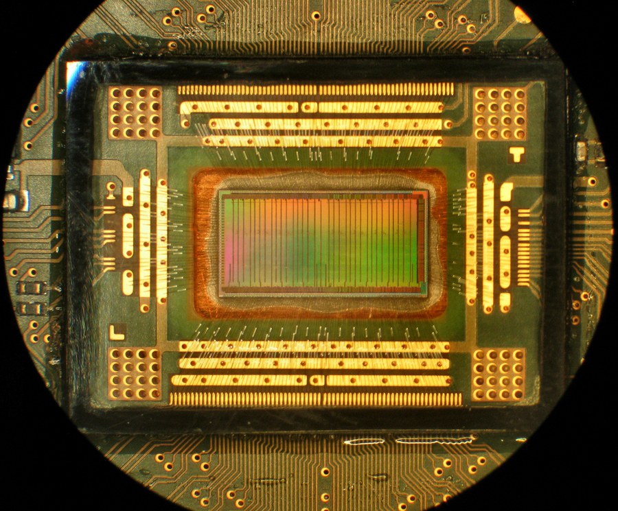
Chipfoto DNC-2 (Chip-on-Board)
| Technologie | 180 nm CMOS |
| Area | 50 mm² |
| Tape-Out | 05_2011 |
MAPLE_Chip
Neuromorphic chip with 16 neurons and 512 synapses operating at a speed-up of 10000, realized in OTA-C circuit technique. Features short-term plasticity and local correlation plasticity (LCP) rule for long-term learning.
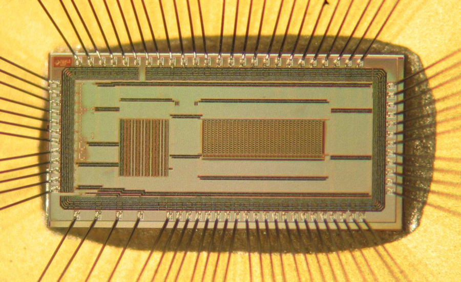
Chipfoto MAPLE_Chip
| Technologie | 180 nm CMOS |
| Area | 4,5 mm² |
| Tape-Out | 07_2011 |
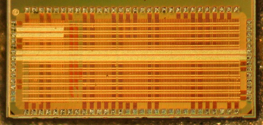
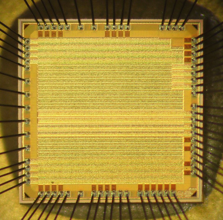
Cool28_SoC
Component test chip for standard cells, high-speed IO cells, and SRAM macros developed at HPSN. Tensilica DSP with adaptive voltage and frequency scaling (AVFS) and corresponding ADPLL clock generator.

Chipfoto, Cool28_SoC
| Technologie | 28 nm CMOS |
| Area | 2,25 mm² |
| Tape-Out | 7_2012 |
| Publikation | DOI: 10.1109/TCSII.2013.2278123 |
Delta-Sigma-ADC
Cooperation with former ZMDI to investigate high resolution incremental delta-sigma ADCs for DC-input signals. It contains two hybrid ADCs with current input and 3 discrete time ADCs with modulators of 3rd and 4th order. The main part of the chip area is filled with photo-diode test structures to evaluate spectral sensitivity of this technology.

Chipfoto Delta-Sigma-ADC
| Technologie | 180 nm CMOS |
| Area | 25 mm² |
| Tape-Out | 10_2012 |
| Publikationen | DOI: 10.1109/ECCTD.2013.6662252 DOI: 10.1109/ISCAS.2013.6572081 DOI: 10.1109/ICECS.2013.6815476 |
TITAN
Testchip with ADPLL, SAR ADC and serial NOC links. Also includes a neuromorphic array with 64 neurons and 8192 plastic synapses and circuits for high resolution on-chip IR measurement. 12 bit 4 MSamples/s SAR ADC with configurable redundancy.
Chipfoto Titan (Multiproject-Chip; eigener Anteil)
| Technologie | 28 nm CMOS |
| Area | 4,5 mm² |
| Tape-Out | 11_2012 |
| Publikationen | DOI: 10.1109/JSSC.2014.2381637 DOI: 10.1109/TBCAS.2014.2379294 |
Tomahawk_2
Heterogeneous MPSoC with 8 Duo processing elements for software defined radio. Fine-grained power management via DVFS. On-chip serial links with up to 72 Gbit/s, DDR2 and FPGA interfaces for off-chip communication.

Chipfoto Tomahawk_2_Chip
| Technologie | 65 nm CMOS |
| Area | 36 mm² |
| Tape-Out | 04_2013 |
| Publikation | DOI: 10.1109/ISSCC.2014.6757394 |
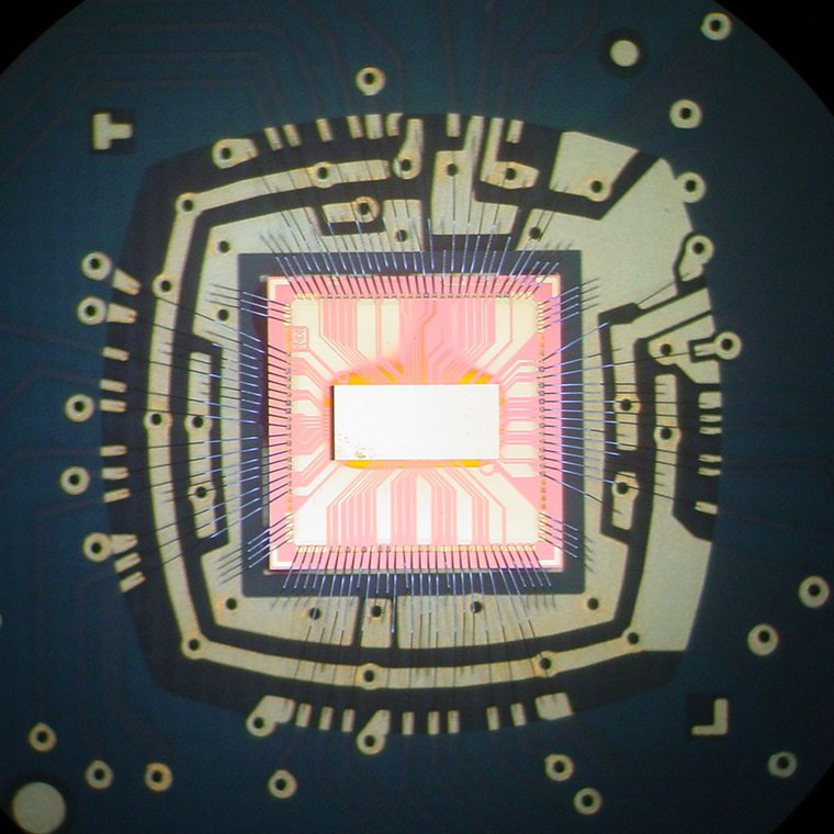
BIONECT_Chip
Neuromorphic chip with 320 neurons for real-time coupling with neural tissue. Contains 1600 conductance-based multi-synapses, enabling emulation of up to 320000 single synaptic connections. Realized in switched-capacitor circuit technique. Short-term plasticity circuits on chip as well.
Chipfoto BIONECT_Chip
| Technologie | 180 nm CMOS |
| Area | 50 mm² |
| Tape-Out | 12_2013 |
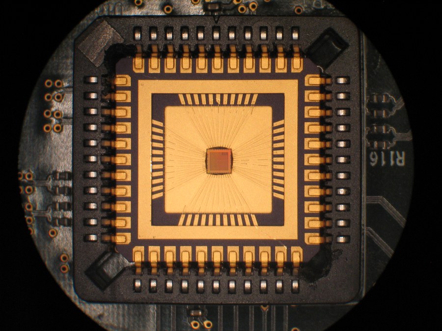
Blizzard_Chip
On-chip DC-DC voltage converter and Tensilica Xtensa DSP with adaptive power management. 10bit 16MS/s SAR ADC with window functionality and PWM signal generator with 62.5ps timing resolution for fast changes of operation modes and high power efficiency.
Chipfoto BLIZZARD_Chip
| Technologie | 28 nm CMOS |
| Area | 4 mm² |
| Tape-Out | 01_2014 |
| Publikationen | DOI: 10.1109/ISCAS.2015.7168989 DOI: 10.1007/s10470-015-0591-2 |
TITAN_3D
Testchip for energy efficient TSV transceiver for 3D chip stacking achieving 50 fJ/Bit at 8 Gbit/s. Flip chip package and custom silicon interposer with redistribution layer. LX5 Tensilica core with instruction set extension optimized for database query processing.
TITAN_3D_Chip_on_Board
| Technologie | 28 nm CMOS |
| Area | 4,5 mm² |
| Tape-Out | 04_2014 |
| Publikationen |
DOI: 10.1007/978-3-319-20481-9_3 |
Tomahawk DBA
Heterogeneous MPSoC with 4 Tensilica ASIPs for database query processing. NoC with 80 Gbit/s serial link. 2 LPDDR2 memory interfaces and off-chip FPGA interface with 5 Gbit/s SerDes links.

Tomahawk_DBA_Chip_on_board
| Technologie | 28 nm CMOS |
| Area | 18 mm² |
| Tape-Out | 10_2014 |
| Publikation | DOI: 10.1145/2897937.2897986 |
Nanolink_65
Testchip for the serial communication links of the neuromorphic BrainScales wafer-scale system within the Human Brain Project (HBP). It contains 2 source-synchronous serial links for chip-to-FPGA communication at data rates up to 2GBit/s.
NanoLink65_CiP
| Technologie | 65 nm CMOS |
| Area | 2,5 mm² |
| Tape-Out | 10_2014 |
Nanolink_28
Testchip for the serial communication links of the neuromorphic many-core system Spinnaker2 within the Human Brain Project (HBP). It contains 2 multi-standard SerDes PHYs with data rates up to 5GBit/s.
Chipfoto NanoLink_28
| Technologie | 28 nm CMOS |
| Area | 2 mm² |
| Tape-Out | 12_2014 |
Santos
Heterogeneous MPSoC with 4 Duo-PEs and fine-grained power management. OpenMSP430 core with timing detection flip-flops for resilient low-power operation in all process corners. ADPLLs enable NoC with GALS clocking scheme and are used as an entropy source for true random number generation.
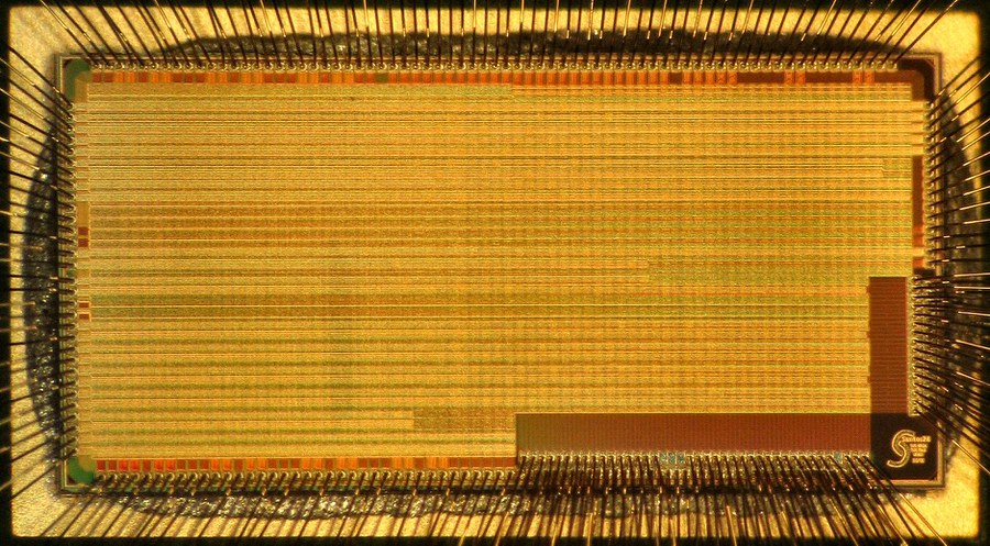
Chipfoto, Santos
| Technologie | 28 nm CMOS |
| Area | 18 mm² |
| Tape-Out | 07_2015 |
| Publikation | DOI: 10.1145/3061639.3062188 |
| <-2006 - 2010 | 2016 - 2020 -> |