Chipentwürfe 2006 bis 2010
Inhaltsverzeichnis
Active-Pixel-Sensor 65
Active sub-100nm pixel image sensor with photo diodes in varying depths in the substrate (116*128 and 48*96 pixels). Also used as a test chip for Delta-Sigma modulator, pipeline ADC, and pixel matrix readout.
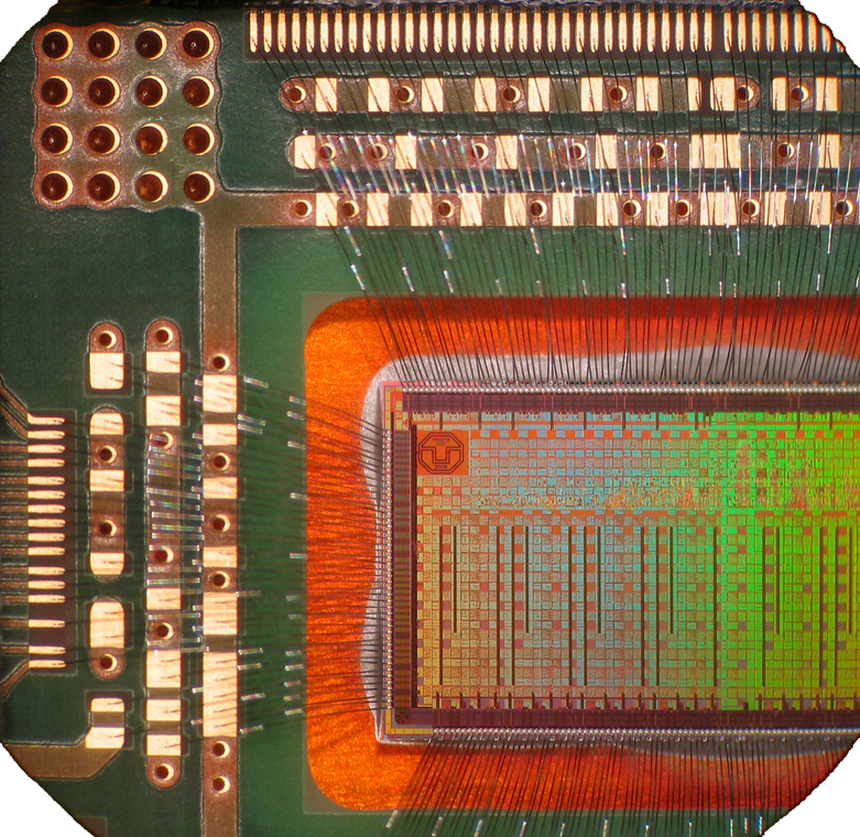
Chipfoto Active-Pixel-Sensor 65
| Technologie | 65 nm CMOS |
| Area | 1,08 mm² |
| Tape-Out | 01_2006 |
Tomahawk 1
Heterogeneous MPSoC for SDR applications. Complete backend implementation at HPSN.
| Technologie | 130 nm CMOS |
| Area | 100 mm² |
| Tape-Out | 03_2007 |
| Publikation | DOI: https://doi.org/10.1109/ESSCIRC.2008.4681893 |
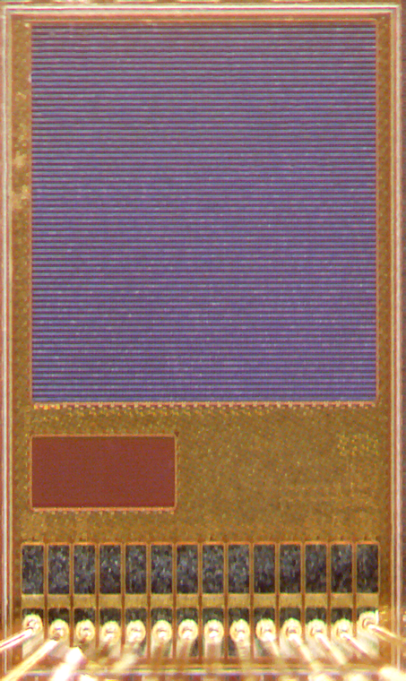
PIXSTACK
High-Speed Image Sensor with 320x240 Pixel cells. Grayscale image with 8bit resolution and 500 frames/s. Power consumption of 50mW at 3.3V supply voltage.
Chipfoto, Pixstack
| Technologie | 0,35 µm CMOS |
| Area | 20 mm² |
| Tape-Out | 06_2007 |
MiniLink
Minilink is series of prototype chips for application-specific digital neuromorphic communication. They contain multiple LVDS source synchronous transmission links, 1GHz PLL and bias generation.

Layout MiniLink_1
| Technologie | 180nm CMOS |
| Area | 4,5 mm² |
| Tape-Out | 06_2007 |

MiniLink_2 Chip_on_Board
| Technologie | 180nm CMOS |
| Area | 2,25 mm² |
| Tape-Out | 01_2008 |

Chipfoto MiniLink_3
| Technologie | 180nm CMOS |
| Area | 2,25 mm² |
| Tape-Out | 04_2008 |

MiniLink_4 Chip_on_Board
| Technologie | 180nm CMOS |
| Area | 4,5 mm² |
| Tape-Out | 06_2008 |
| Minilink- Publikationen |
DOI:10.1016/j.vlsi.2011.05.003 DOI: 10.3389/fnins.2011.00117 |
AFE_Chip
Programmable gain amplifier (PGA) and Delta-Sigma modulator (DSM) for automotive applications. The DSM is realized in switched-capacitor in a MASH 2-1-1 structure. Also incorporates student-designed OTA circuits.
Chipfoto AFE_Chip
| Technologie | 0,6 µm CMOS |
| Area | 21,16 mm² |
| Tape-Out | 08_2008 |
| Publikation | https://ieeexplore.ieee.org/document/5551697 DOI: 10.1109/ICECS.2009.5410940 |
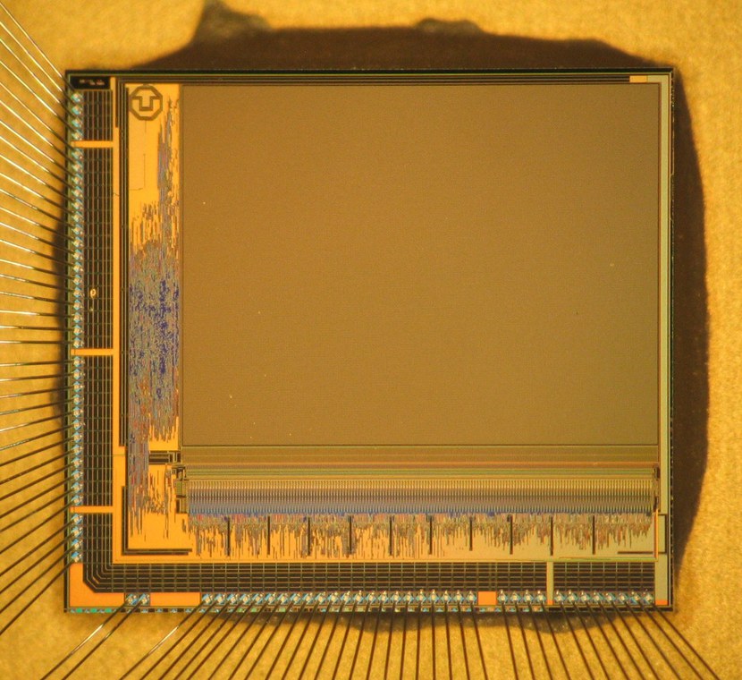
DNC_Chip
High-speed pulse transmission and routing chip for the first-generation BrainScales waferscale system. Hosts 8 serial LVDS links to neuromorphic chips and one multi-lane FPGA interface for a total throughput of 32Gbit/s.
Chipfoto DNC_Chip (Detail)
| Technologie | 180 nm CMOS |
| Area | 50 mm² |
| Tape-Out | 11_2008 |
| Publikationen |
www.sciencedirect.com/../article/../S0167926011000538 |
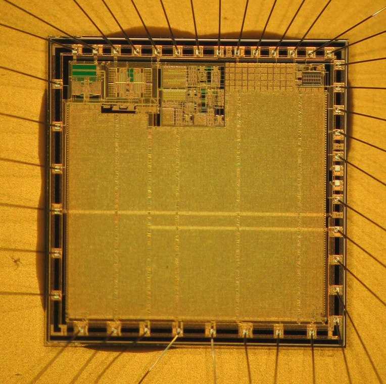
TOMMY_Chip
MPSoC with MIMO sphere decoder and FEC for mobile baseband processing. GALS clocking using 8 ADPLLs, packet-oriented NoC, and LVDS FPGA interface.

Chipfoto TOMMY_Chip (im Package)
| Technologie | 65 nm CMOS |
| Area | 7,4 mm² |
| Tape-Out | 03_2010 |
| Publikationen |
DOI: 10.1109/ISSCC.2012.6176981 |
| <- bis 2005 | 2011 - 2015 -> |