
IC designs 2016 - 2020
Table of contents
AUTOLINK_28
Autolink28 is an Ethernet physical layer test chip that complies with the 1000BASE-T1 Ethernet standard. It includes a physical coding sublayer (PCS) and a physical medium attachment (PMA) on the transmit (TX) and receive (RX) sides, respectively, and achieves a symbol rate of up to 750 Mbps in full-duplex mode.
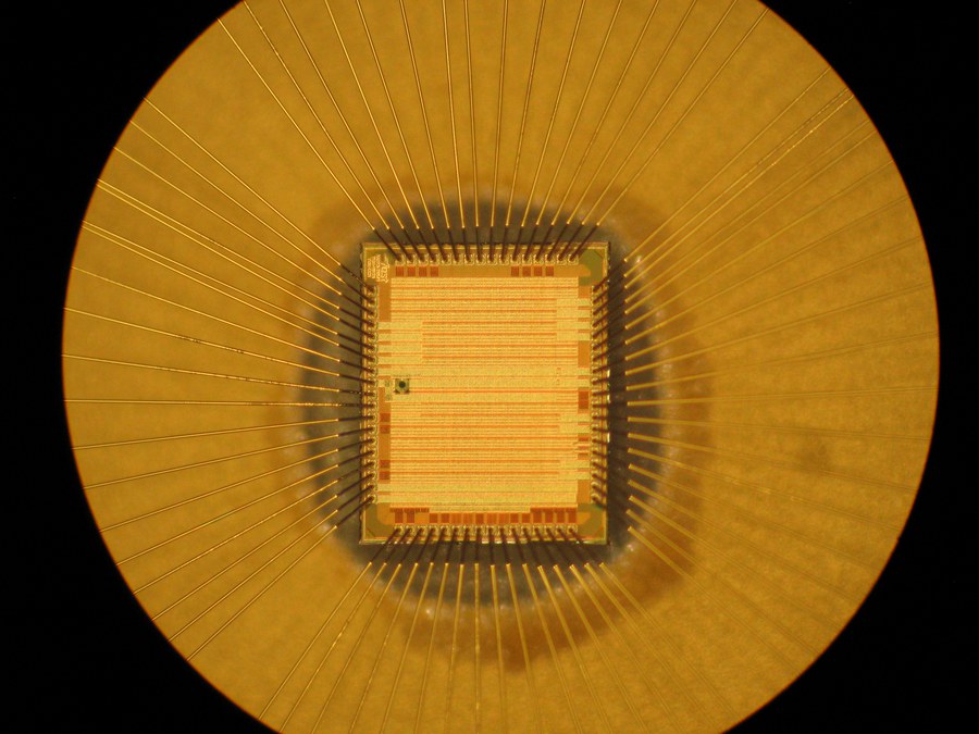
Chipfoto Autlink_28-IC
| Technology | 28 nm CMOS |
| Area | 2.75 mm² |
| Tape-out | September 2016 |
| Publications | doi: 10.1109/ISCAS.2019.8702118 |
JIB_1
JIB1 is the first prototype of the quad processing unit (QPE) architecture and layout for the SpiNNaker2 chip. JIB1 contains two QPEs, for a total of 8 processing elements. Each processing element features a multiply-accumulate array for deep neural networks, log, exp, and random function generators for spiking neural networks, and an ARM M4F core. All numerical units incorporate dynamic voltage and frequency scaling, meaning that power consumption and clock frequency scale with the chip’s computational activity. The chip includes other system components for the final SpiNNaker2 chip, such as the updated SpiNNaker router, a DMA engine, custom high-speed on-chip and off-chip communication links, and more.
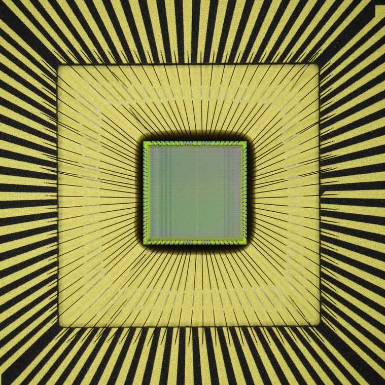
Chipfoto JIB1-IC
| Technology | 22 nm FDSOI |
| Area | 9 mm² |
| Tape-out |
March 2018 |
|
Supported by the European Union’s 7th Framework Program and Horizon 2020 Framework |
|
Kachel
Cooperation with MNS, MPSoC with 4 cores and fine-grained power management. Single-ended 2 Gbit/s/lane chip-to-chip links to extend the NoC to neighboring chips.
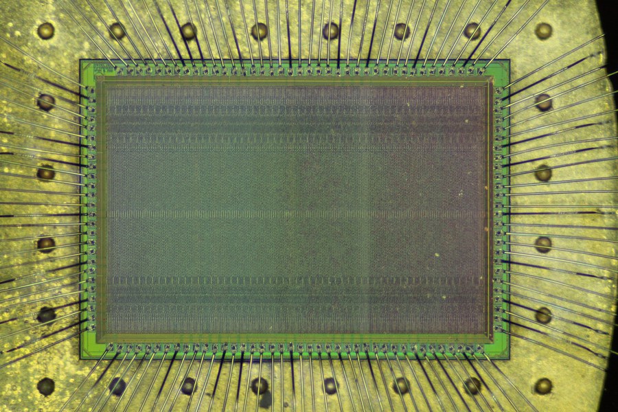
Chipfoto Kachel-IC
|
Technology |
22 nm FDSOI |
| Area | 8.4 mm² |
| Tape-out |
May 2018 |
Kachel_2
Collaboration with MNS, MPSoC with 11 cores and fine-grained power management. Single-ended 2 Gbit/s per lane chip-to-chip links to extend the NoC to neighboring chips.
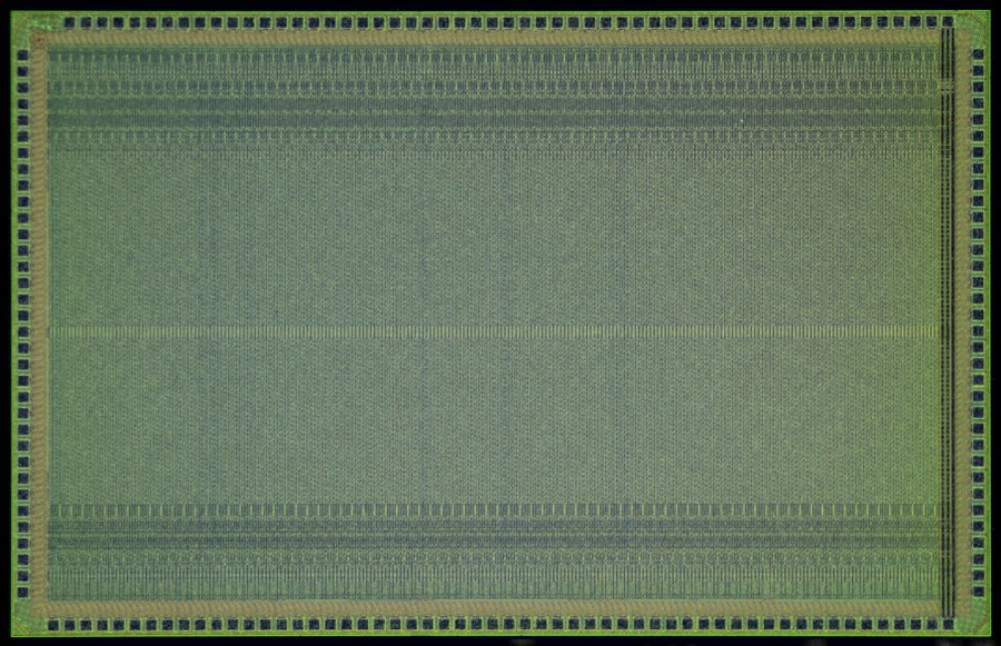
Chipfoto Kachel2-IC
|
Technology |
22 nm FDSOI |
| Area | 14.5 mm² |
| Tape-out |
February 2019 |
GEPARD
Smart neural SoC featuring a MAC-assisted CPU, 16-channel AFE, bio-processing accelerator, and ABB unit. The proposed SoC achieves an average classification accuracy of 94.12% and power consumption of 2.79 μW/ch for the classification and 1.52 μW/ch for the AFE. Various architecture- and circuit-level techniques are employed to achieve ultra-low-power operation.
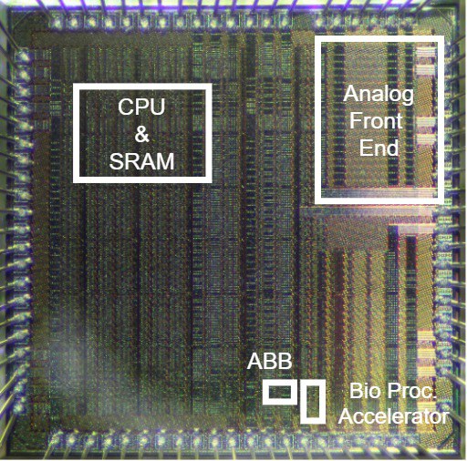
Chipfoto GEPARD-IC
|
Technology |
22 nm FDSOI |
| Area | 4 mm² |
| Tape-out |
June 2019 |
| Publications |
DOI: 10.1109/TCSII.2021.3121034 |
IPCEI_ADC-test
Test chip of a dual ADC macro for the IPCEI Radar DSP.
The dual ADC macro contains two SAR ADCs with 12-bit resolution and a sampling rate of 28 MSamples/s, used for synchronous sampling of the I and Q components of the IF signals from the radar front end.
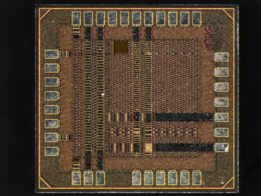
Chipfoto IPCEi ADC-Test-IC
|
Technology |
22 nm FDSOI |
| Area | 1.56 mm² |
| Tape-out |
August 2019 |
JIB_2
JIB2 is the second (and final) prototype of the quad processing unit (QPE) architecture and layout for the SpiNNaker2 chip. Its goal is to verify all the macros in their final layouts that will make up SpiNNaker2 through silicon verification. Thus, it contains the final versions of the QPEs with all the machine learning and neuromorphic functionality described for JIB1, plus the layouts of the LPDDR4 interfaces. It is also intended to test the final package and interposer design, so it is actually housed in the same package as SpiNNaker2. JIB2 contains: 2 QPEs (i.e., 8 PEs), chip-to-chip links, board-to-board links, an Ethernet host interface, the final SpiNNaker2 event router, etc. Fun fact: In the picture, the mirror-like element in the middle is actually the backside of the JIB2 die—that is, the silicon chip itself. In this package, the backside of the die protrudes from the top surface.
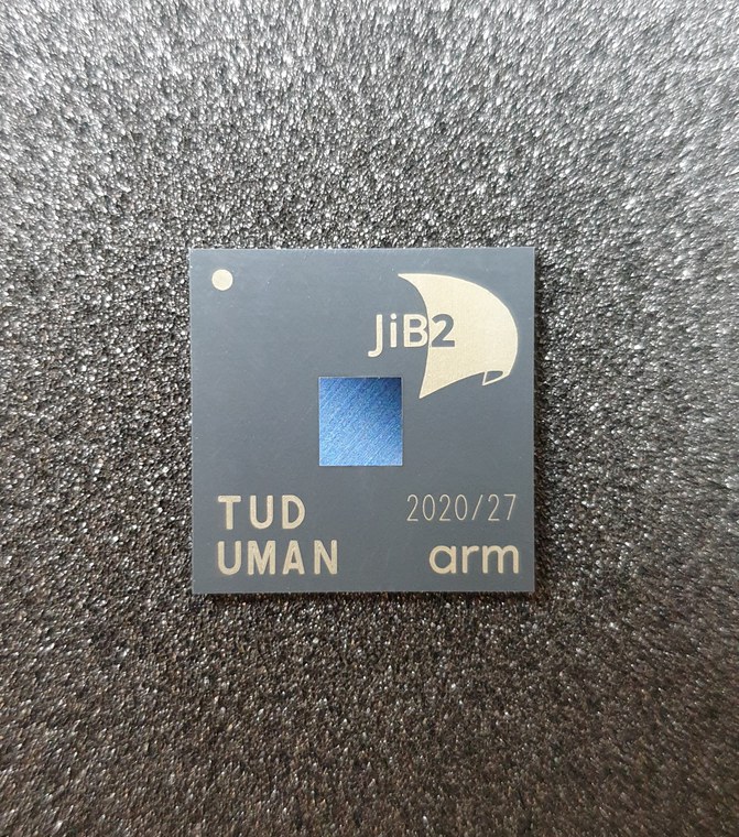
Chipfoto JIB2-IC (BGA-Package)
|
Technology |
22 nm FDSOI |
| Area | 19.8 mm² |
| Tape-out |
March 2020 |
| Supported by the European Union’s 7th Framework Program and Horizon 2020 Framework Programs, under grant agreements 720270, 785907 (HBP) |
|
IPCEI DSP
DSP for a MIMO (4Tx/6Rx) FMCW radar to perform 4D localization and identification of targets using on-chip machine learning in automotive applications. The DSP features 24 RISC-V-based PEs, each equipped with MAC and FFT accelerators to handle the real-time processing demands of the IQ intermediate frequency signals received from 12 ADCs. The FFT accelerator is a variable-length, dual-radix accelerator optimized to handle resolution changes within the radar processing chain and designed for a multi-core topology thanks to its compact footprint. The four LVDS lines on the chip also enable the extraction of raw data recordings. The 24 application PEs are interconnected in a lightweight network-on-chip with full access to all resources (e.g., ADCs, LVDS, GPIOs, serial interfaces) and to a management PE located at the periphery. The chip as a whole uses forward body bias (FBB) at a nominal supply voltage of 0.6 V in 22FDX technology and ball grid array (BGA) as its surface-mount packaging.
|
Technology |
22 nm FDSOI |
| Area | 15 mm² |
| Tape-out |
October 2020 |
| Publications | DOI: 10.1109/ISCAS51556.2021.9401547 DOI: 10.1049/rsn2.12063 DOI: 10.1109/RWS50353.2021.9360348 DOI: 10.1109/RADAR41533.2019.171412 |
| <- 2011 - 2015 |