Project A10: System Integration for Optical and Wireless Pbit/s Communication in High Performance Computing
The main research focus of the project is the integration of components of communication transceivers into the high performance package. The work program is divided into two research areas: electro-optical integration and packaging for mm-wave communication. Embedding and integration of link components on the wafer-level will be investigated in order to support the 3D stacking. For high pin count, optical I/O wafer-level coupling optics will be developed. To address the new integrated photonic devices, the re-development of onboard integrated waveguides (single mode, telecom wavelengths) will be addressed.
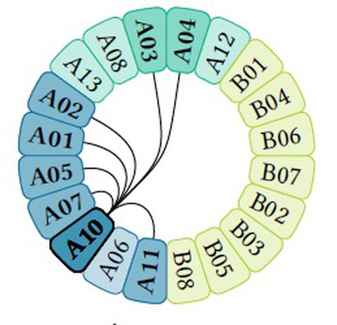
Role within the CRC 912
A01:
o Share of 130 nm SiGe BiCMOS technology, model evaluation and overall design flow experience/know-how
o Share of device characterization infrastructure
o DC board design, assembly and testing
A02:
o Evaluation of FPGA use for connection of the optical demonstrator with the HAEC playground
A04:
o Discussion and exchange of optical link performance parameters, specifications and component geometries for modeling the optical connection in the HAEC Box
A06:
o Lab support for measuring the 100 Gb/s TIA
A10:
o Work on optical VCSEL-based demonstrator concept and setup
A11:
o Discussion about co-integration of modulator and driver designs
o Specification of target parameters for the modulator and driver
B06:
44
o Discussions on and exchange of optical link IC parameters and conditions for developing a stochastic model to estimate the
Staff
Principal Investigator
Postdoc
Technicians

